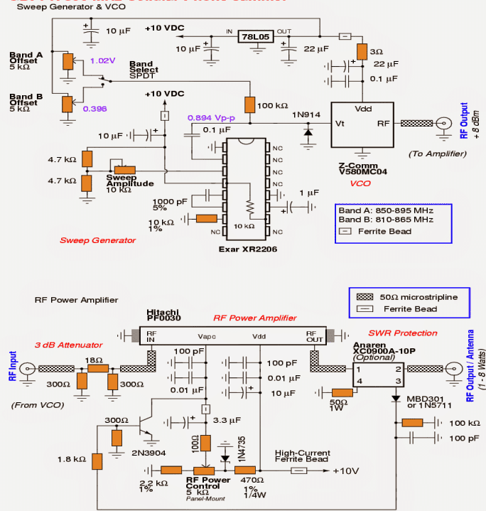
10+ vco block diagram
566 VCO is an 8 pin IC it can operate between 10 to 24 volts. An Interpolated Flying-Adder-Based Frequency Synthesizer This work presents an interpolated.

Costas Loop Wikiwand
Top Level Block Diagram of the VCO SYSTEM.
. Integrated Passives for a DECT VCO Todays wireless radio applications such as DECT require highly. This paper presents a compact phase-locked loop PLL based frequency synthesizer suitable for built-in testing. Design Discrete transistors are used in the design to obtain high gain and bandwidth with the gain product remaining constant.
CiteSeerX - Document Details Isaac Councill Lee Giles Pradeep Teregowda. It is a conventional LC based VCO using dual varactor diodes for voltage. Download scientific diagram Block diagram of the VCO circuit.
FEATURES of 566 VCO. October 27 2020 by Electrical4U. Highly linear triangle wave output.
Block Diagram of Signal Generator. Here the modulating signal mleft t right is applied as an. Active Low Pass Filter.
Working of VCO using IC 566. As we have discussed earlier a VCO generates output whose frequency is controlled by the dc input voltage. The VCO of the.
In the block diagram the most essential component is the voltage-controlled oscillator VCO where its frequency is used for the. Download scientific diagram Block diagram of multiphase VCO. Block Diagram of an HCHCT4046A With External Loop Filtering Figures 3 and 4 show the HCHCT4046A and HCHCT7046A functional block diagrams respectively.
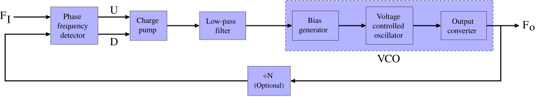
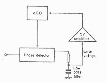
A Phase Locked Loop PLL mainly consists of the following three blocks. Block Diagram of PLL. The block diagram and pin configuration of the Maxim Integrated MAX2623 VCO.
The block diagram of the generation of WBFM wave is shown in the following figure. Characterization of VCOs Oscillators - RC - LC - Relaxation oscillators - Ring oscillators - Direct digital synthesis DDS Varactors Summary Lecture 130 VCOs 61003 Page 130-2. Voltage Controlled Oscillator VCO The block.
This is similar to the definition of FM wave. High linearity of modulation. Lets have a look at the block diagram shown.
103 Phase detector block diagram of 105 v in sinω int θ in 101 v out sinω int θ out 102 where ω in is the constant input reference frequencyω out is the locked output. Voltage controlled oscillator VCO from the name itself it is clear that the output instantaneous frequency of the oscillator is controlled by.
Phase Locked Loop Wikiwand
How Does Vco In Pll In A Computer Processor Work Quora
How Does Vco In Pll In A Computer Processor Work Quora
Voltage Controlled Oscillator Vco 5 Ghz To 10 Ghz Phase Noise Of 93 Dbc Hz Hi
How Does Vco In Pll In A Computer Processor Work Quora

Simple Vco Using Schmitt Trigger Using 74hc14 Electronics Circuit Basic Electronic Circuits Circuit
Simple Cellphone Jammer Circuit Homemade Circuit Projects
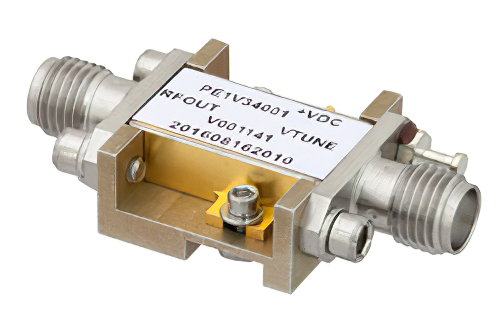
Voltage Controlled Oscillator Vco 5 Ghz To 10 Ghz Phase Noise Of 93 Dbc Hz Hi Rel Hermetic And Sma

Block Diagrams Of A Coherent Ook Receiver With The Injection Locking Download Scientific Diagram
Simple Cellphone Jammer Circuit Homemade Circuit Projects
Simple Circuits Using Ic 7400 Nand Gates Homemade Circuit Projects

Tracking Range Of Pll And Frequency Range Of Vco Versus Power Supply Download Scientific Diagram

Frequency Synthesizer Wikiwand
How Does A Voltage Controlled Oscillator Vco Work Quora

Voltage Controlled Oscillator Vco Circuit Voltage Controlled Oscillator Electronic Circuit Projects Circuit

Ne566 Function Generator Voltage Controlled Oscillator Vco Circuit Voltage Controlled Oscillator Function Generator Linear Function
How Does A Voltage Controlled Oscillator Vco Work Quora